B.Tech. Electronics and Communication Engineering (VLSI Design and Technology)
- Hands-on Training
- Faculty with International Experience
- Advanced Curriculum
- Upto 100% Scholarship based on merit

About the Course
The Electronics and Communication Engineering (ECE) program at Takshashila University stands out for its innovative education delivery methodology and well-structured academic framework, designed by distinguished academicians, researchers, and industry experts. The curriculum effectively integrates core areas such as science, mathematics, engineering, and technology with humanities, professional ethics, and industry-oriented practices, ensuring that students evolve into competent, industry-ready professionals over the span of four years.
To further enhance career opportunities in emerging domains, the program is designed to provide a strong academic foundation and flexibility for pursuing higher studies and specialization in advanced areas of Electronics and Communication Engineering. The curriculum equips students with essential analytical, technical, and problem-solving skills, enabling them to address complex challenges in communication and technology. It also prepares graduates to pursue postgraduate programs, research opportunities, and professional careers in globally evolving and industry-driven environments.
SCOPE OF THE PROGRAMME
The programme offers in-depth knowledge in VLSI design and technology, covering areas such as digital design verification, analog and mixed-signal design, RTL design and synthesis, and electronic design automation. Graduates will be well-prepared to pursue careers in industries related to semiconductor design, electronics manufacturing, and advanced computing systems.
Course Curriculum

Year 1 (Foundation Stage)
The first year focuses on building a strong foundation in engineering fundamentals. Students are introduced to mathematics, physics, and basic electrical and electronics concepts along with programming skills essential for understanding hardware design and simulation tools.
Key Subjects: Mathematics, Physics, Basic Electrical Engineering, Engineering Graphics, Programming in C/Python, Electronic Devices and Circuits
Second Year (Core Electronics & Communication Fundamentals)
In the second year, students develop core knowledge in electronics and semiconductor physics, which are essential for VLSI design. They learn circuit analysis, digital logic, and the behavior of semiconductor devices used in integrated circuits.
Key Subjects: Analog Electronics, Digital Electronics, Network Theory, Signals and Systems, Semiconductor Devices, Electromagnetic Fields, Probability and Random Processes
Third Year (VLSI Design & Hardware Systems)
The third year emphasizes VLSI design concepts and hardware system development. Students gain practical knowledge in designing integrated circuits, understanding CMOS technology, and using industry-relevant tools. Mini-projects and design-based learning are key components at this stage.
Key Subjects: VLSI Design, CMOS Technology, Digital System Design, Microprocessors and Microcontrollers, Embedded Systems, FPGA-Based System Design, Electronic Design Automation (EDA) Tools
Fourth Year (Advanced VLSI & Industry Readiness)
In the final year, students focus on advanced VLSI topics and real-time applications. They work on industry-oriented projects, gain exposure to chip design flow, and explore emerging areas in semiconductor technology and system-on-chip (SoC) design.
Key Subjects: ASIC Design, System-on-Chip (SoC) Design, Physical Design and Verification, Low Power VLSI Design, Testing and Validation of ICs, Nanoelectronics, Project Work / Internship.
Programme Educational Objectives (PEOs)
Upon completing the B.Tech. Electronics and Communication Engineering (VLSI Design and Technology), you will have gained the following competencies:
PEO1: Engineering Knowledge and Problem Solving
Graduates will apply knowledge of mathematics, basic sciences, and engineering principles to analyze and solve complex problems in VLSI systems with consideration for societal and environmental needs.
PEO2: Design and Development of VLSI Systems
Graduates will design, develop, and test analog and digital integrated circuits using modern tools to meet industry requirements and technological advancements.
PEO3: Professional Skills and Teamwork
Graduates will demonstrate professional competence by working effectively in multidisciplinary teams, exhibiting leadership, ethical practices, and effective communication skills.
PEO4: Lifelong Learning and Career Development
Graduates will pursue higher education, research, and lifelong learning to adapt to emerging technologies and achieve sustained career growth in VLSI and related domains.
Programme Outcomes (POs)
The B.Tech. Electronics and Communication Engineering (IOT) will help you achieve the following broader learning outcomes:
PO1: Engineering Knowledge
Apply knowledge of mathematics, science, engineering fundamentals, and specialization to solve complex engineering problems.
PO2: Problem Analysis
Identify, formulate, review research literature, and analyze complex engineering problems using first principles.
PO3: Design / Development of Solutions
Design solutions for complex engineering problems considering public health, safety, and societal needs.
PO4: Conduct Investigations of Complex Problems
Use research-based knowledge, design experiments, analyze data, and derive valid conclusions.
PO5: Modern Tool Usage
Select and apply appropriate modern engineering and IT tools for modeling, simulation, and problem-solving.
PO6: The Engineer and Society
Apply contextual knowledge to assess societal, legal, health, and safety issues in engineering practice.
PO7: Environment and Sustainability
Understand environmental impact and apply principles of sustainable development.
PO8: Ethics
Apply ethical principles and commit to professional ethics and responsibilities.
PO9: Individual and Team Work
Function effectively as an individual and as a member/leader in multidisciplinary teams.
PO10: Communication
Communicate effectively through reports, presentations, and professional interactions.
PO11: Project Management and Finance
Apply engineering and management principles to manage projects in multidisciplinary environments.
Programme Specific Outcomes (PSOs)
Through this programme, you will develop the following specific competencies:
PSO1: VLSI Design and Analysis
Apply the knowledge of analog and digital VLSI design principles to analyze, design, and implement integrated circuits and electronic systems for real-world applications.
PSO2: Modern Tools and Technologies
Utilize modern engineering tools, hardware, and software (EDA tools) for modeling, simulation, and development of semiconductor devices and VLSI systems.
PSO3: Innovation and Societal Applications
Develop innovative, efficient, and sustainable VLSI-based solutions with consideration for environmental impact, societal needs, and emerging technological advancements.
Career Scope
Graduates of the BB.Tech. Electronics and Communication Engineering (IOT) are prepared for a wide range of roles in the electronics and telecommunications industries. Career opportunities include:
VLSI Design Engineer
- Role:Design and develop integrated circuits (ICs) and semiconductor chips for applications in consumer electronics, communication systems, and computing devices.
- Salary: ₹6,00,000 to ₹15,00,000 per annum
Physical Design Engineer
- Role: Work on chip layout design, placement, routing, and optimization to ensure performance, power efficiency, and manufacturability.
- Salary: ₹5,00,000 to ₹14,00,000 per annum
Verification Engineer
- Role:Test and validate VLSI designs using simulation and verification tools to ensure functionality and reliability before fabrication.
- Salary:₹5,00,000 to ₹13,00,000 per annum
Analog Design Engineer
- Role:Design analog circuits such as amplifiers, oscillators, and power management systems used in ICs.
- Salary: ₹6,00,000 to ₹14,00,000 per annum
FPGA Design Engineer
- Role:Develop and implement digital systems using FPGA platforms for rapid prototyping and hardware acceleration.
- Salary:₹5,00,000 to ₹12,00,000 per annum
Embedded Systems Engineer
- Role: Design and program embedded hardware systems integrated with VLSI chips for applications like automotive, IoT, and consumer electronics.
- Salary: ₹5,00,000 to ₹12,00,000 per annum
EDA Tool Engineer
- Role:Develop and maintain Electronic Design Automation (EDA) tools used for chip design, simulation, and verification.
- Salary:₹6,00,000 to ₹16,00,000 per annum
Semiconductor Process Engineer
- Role: Work on fabrication processes, material technology, and manufacturing of semiconductor devices.
- Salary: ₹5,00,000 to ₹12,00,000 per annum
Research and Development Engineer
- Role:Engage in advanced research in VLSI, nanoelectronics, and next-generation semiconductor technologies.
- Salary: ₹6,00,000 to ₹18,00,000 per annum
Why TAKSHASHILA?

Industry-Relevant Curriculum
The B.Tech programme is crafted to meet the latest industry requirements, ensuring students gain up-to-date knowledge and skills in electronics and communications engineering.
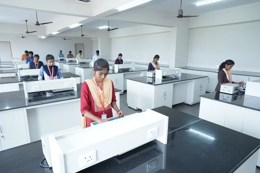
Hands-On Experience
You will work with modern tools and technologies in state-of-the-art laboratories, gaining practical experience that directly applies to industry demands.
Expert Faculty
Learn from distinguished faculty members with years of academic and industry experience.
Global Career Opportunities
Takshashila University’s global network of partners and industry contacts will help you access career opportunities worldwide.

- Applicants must have completed their 10+2 or equivalent in Science with a minimum of 50% marks, including subjects like Physics, Chemistry, and Mathematics.
- Entrance exams or personal interviews may be required as part of the selection process.

For All Programmes except MBA, MCA, M.Tech, and Integrated Programmes offered by Sunstone, FacePrep, Kalvium and NxtWave
|
S.No |
% of Marks |
Scholarship Amount in Tuition Fees per year |
|
1 |
60% – 75% |
10% |
|
2 |
Above 75 % – 90 % |
25 % |
|
3 |
Above 90 % |
50 % |
Calculation of percentage of Marks (+2 of HSC / 2nd Year of APBIM or +2 of CBSE or Equivalent)
- Engineering – Average marks in Mathematics, Physics, Chemistry/Computer Science
- Lateral Entry – Average marks in Diploma Programme.
- Agriculture – Average marks in Physics, Chemistry, Biology / Botany &Zoology
- AHS / BPT / Pharmacy – Average marks in Physics, Chemistry, Biology / Botany &Zoology/Bio Tech
- UG – Arts & Science / Hotel Management – Overall +2 marks – (+2 of HSC / 2nd Year of APBIM or +2 of CBSE or Equivalent)
- PG – Overall % in UG
- Diploma – Average mark in 10th /Equivalent
MBA, MCA, M. Tech, and Integrated Programmes offered by Sunstone, FacePrep, Kalvium and NxtWave – No Academic Scholarship applicable.
Spread over 150 acres
At Takshashila University, you will have ample opportunities to hone your skills in real-world healthcare settings, utilising state-of-the-art medical facilities and simulation labs on our 150-acre campus.


Start your journey in Electronics & Communications Engineering today!
Frequently Asked Questions (FAQs)
What is the duration of the B.Tech in Electronics & Communications Engineering?
The course lasts for 4 years, divided into eight semesters.
Do I need prior experience in electronics or communications to apply?
No, the course is designed for students with a background in science, specifically in Physics, Chemistry, and Mathematics.
What career support is provided after graduation?
Takshashila University provides job placements, internships, and networking opportunities to help you kickstart your career in electronics and communications engineering.
Is the programme recognised internationally?
Yes, the B.Tech programme aligns with international academic standards, preparing you for global career opportunities in electronics and communication engineering.